- 您现在的位置:买卖IC网 > Sheet目录1905 > ATMEGA644P-B15MZ (Atmel)IC MCU 8BIT 64KB FLASH 32VQFN
PIC16(L)F1826/27
DS41391D-page 244
2011 Microchip Technology Inc.
25.4
I2C
MODE OPERATION
All MSSPx I2C communication is byte oriented and
shifted out MSb first. Six SFR registers and 2 interrupt
flags interface the module with the PIC microcon-
troller and user software. Two pins, SDAx and SCLx,
are exercised by the module to communicate with
other external I2C devices.
25.4.1
BYTE FORMAT
All communication in I2C is done in 9-bit segments. A
byte is sent from a Master to a Slave or vice-versa, fol-
lowed by an Acknowledge bit sent back. After the 8th
falling edge of the SCLx line, the device outputting
data on the SDAx changes that pin to an input and
reads in an acknowledge value on the next clock
pulse.
The clock signal, SCLx, is provided by the master.
Data is valid to change while the SCLx signal is low,
and sampled on the rising edge of the clock. Changes
on the SDAx line while the SCLx line is high define
special conditions on the bus, explained below.
25.4.2
DEFINITION OF I2C TERMINOLOGY
There is language and terminology in the description
of I2C communication that have definitions specific to
I2C. That word usage is defined below and may be
used in the rest of this document without explanation.
This table was adapted from the Philips I2C
specification.
25.4.3
SDAX AND SCLX PINS
Selection of any I2C mode with the SSPxEN bit set,
forces the SCLx and SDAx pins to be open-drain.
These pins should be set by the user to inputs by set-
ting the appropriate TRIS bits.
25.4.4
SDAX HOLD TIME
The hold time of the SDAx pin is selected by the
SDAHT bit of the SSPxCON3 register. Hold time is the
time SDAx is held valid after the falling edge of SCLx.
Setting the SDAHT bit selects a longer 300 ns mini-
mum hold time and may help on buses with large
capacitance.
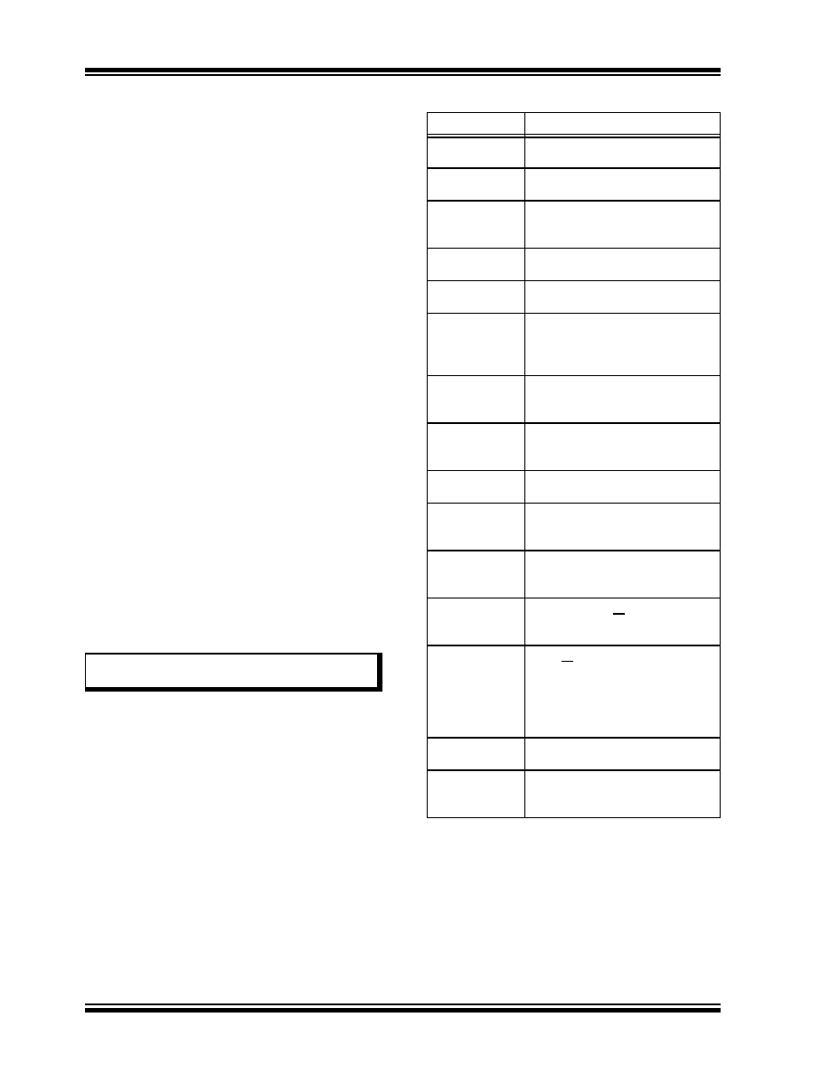
TABLE 25-2:
I2C BUS TERMS
Note:
Data is tied to output zero when an I2C
mode is enabled.
TERM
Description
Transmitter
The device which shifts data out
onto the bus.
Receiver
The device which shifts data in
from the bus.
Master
The device that initiates a transfer,
generates clock signals and termi-
nates a transfer.
Slave
The device addressed by the mas-
ter.
Multi-master
A bus with more than one device
that can initiate data transfers.
Arbitration
Procedure to ensure that only one
master at a time controls the bus.
Winning arbitration ensures that
the message is not corrupted.
Synchronization Procedure to synchronize the
clocks of two or more devices on
the bus.
Idle
No master is controlling the bus,
and both SDAx and SCLx lines are
high.
Active
Any time one or more master
devices are controlling the bus.
Addressed
Slave
Slave device that has received a
matching address and is actively
being clocked by a master.
Matching
Address
Address byte that is clocked into a
slave that matches the value
stored in SSPxADD.
Write Request
Slave receives a matching
address with R/W bit clear, and is
ready to clock in data.
Read Request
Master sends an address byte with
the R/W bit set, indicating that it
wishes to clock data out of the
Slave. This data is the next and all
following bytes until a Restart or
Stop.
Clock Stretching When a device on the bus hold
SCLx low to stall communication.
Bus Collision
Any time the SDAx line is sampled
low by the module while it is out-
putting and expected high state.
发布紧急采购,3分钟左右您将得到回复。
相关PDF资料
ATMEGA644V-10PU
IC AVR MCU FLASH 64K 40DIP
ATMEGA645V-8MI
IC AVR MCU FLASH 64K 1.8V 64QFN
ATMEGA649-16MI
IC AVR MCU FLASH 64K 5V 64QFN
ATMEGA649V-8MI
IC AVR MCU FLASH 64K 1.8V 64QFN
ATMEGA8515L-8JUR
MCU AVR 8KB FLASH 8MHZ 44PLCC
ATMEGA8515L-8PJ
IC MCU AVR 8K 5V 8MHZ 40-DIP
ATMEGA8535-16JUR
MCU AVR 8K FLASH 16MHZ 44PLCC
ATMEGA8535L-8PJ
IC MCU AVR 8K 5V 8MHZ 40-DIP
相关代理商/技术参数
ATMEGA644PR212-AU
功能描述:8位微控制器 -MCU ATmega 644PV-10AU AT86RF212-ZU RoHS:否 制造商:Silicon Labs 核心:8051 处理器系列:C8051F39x 数据总线宽度:8 bit 最大时钟频率:50 MHz 程序存储器大小:16 KB 数据 RAM 大小:1 KB 片上 ADC:Yes 工作电源电压:1.8 V to 3.6 V 工作温度范围:- 40 C to + 105 C 封装 / 箱体:QFN-20 安装风格:SMD/SMT
ATMEGA644PR212-MU
功能描述:8位微控制器 -MCU ATmega 644PV-10MU AT86RF212-ZU RoHS:否 制造商:Silicon Labs 核心:8051 处理器系列:C8051F39x 数据总线宽度:8 bit 最大时钟频率:50 MHz 程序存储器大小:16 KB 数据 RAM 大小:1 KB 片上 ADC:Yes 工作电源电压:1.8 V to 3.6 V 工作温度范围:- 40 C to + 105 C 封装 / 箱体:QFN-20 安装风格:SMD/SMT
ATMEGA644PR231-AU
功能描述:8位微控制器 -MCU ATmega 644PV-10AU AT86RF231-ZU RoHS:否 制造商:Silicon Labs 核心:8051 处理器系列:C8051F39x 数据总线宽度:8 bit 最大时钟频率:50 MHz 程序存储器大小:16 KB 数据 RAM 大小:1 KB 片上 ADC:Yes 工作电源电压:1.8 V to 3.6 V 工作温度范围:- 40 C to + 105 C 封装 / 箱体:QFN-20 安装风格:SMD/SMT
ATMEGA644PR231-MU
功能描述:8位微控制器 -MCU ATmega 644PV-10MU AT86RF231-ZU RoHS:否 制造商:Silicon Labs 核心:8051 处理器系列:C8051F39x 数据总线宽度:8 bit 最大时钟频率:50 MHz 程序存储器大小:16 KB 数据 RAM 大小:1 KB 片上 ADC:Yes 工作电源电压:1.8 V to 3.6 V 工作温度范围:- 40 C to + 105 C 封装 / 箱体:QFN-20 安装风格:SMD/SMT
ATMEGA644PV-10AQ
功能描述:8位微控制器 -MCU AVR 64KB, 2KB EE 20MHz 4KB SRAM, 1.8V RoHS:否 制造商:Silicon Labs 核心:8051 处理器系列:C8051F39x 数据总线宽度:8 bit 最大时钟频率:50 MHz 程序存储器大小:16 KB 数据 RAM 大小:1 KB 片上 ADC:Yes 工作电源电压:1.8 V to 3.6 V 工作温度范围:- 40 C to + 105 C 封装 / 箱体:QFN-20 安装风格:SMD/SMT
ATMEGA644PV-10AQR
功能描述:8位微控制器 -MCU AVR 64KB FLSH 2KB EE 4KB SRAM-20MHz, 5V RoHS:否 制造商:Silicon Labs 核心:8051 处理器系列:C8051F39x 数据总线宽度:8 bit 最大时钟频率:50 MHz 程序存储器大小:16 KB 数据 RAM 大小:1 KB 片上 ADC:Yes 工作电源电压:1.8 V to 3.6 V 工作温度范围:- 40 C to + 105 C 封装 / 箱体:QFN-20 安装风格:SMD/SMT
ATMEGA644PV-10AU
功能描述:8位微控制器 -MCU AVR 64K FLASH 2K EE 4K SRAM ADC-10MHZ RoHS:否 制造商:Silicon Labs 核心:8051 处理器系列:C8051F39x 数据总线宽度:8 bit 最大时钟频率:50 MHz 程序存储器大小:16 KB 数据 RAM 大小:1 KB 片上 ADC:Yes 工作电源电压:1.8 V to 3.6 V 工作温度范围:- 40 C to + 105 C 封装 / 箱体:QFN-20 安装风格:SMD/SMT
ATMEGA644PV-10AUR
功能描述:8位微控制器 -MCU AVR 64KB FLSH 2KB EE 4KB SRAM-10MHz, 1.8V RoHS:否 制造商:Silicon Labs 核心:8051 处理器系列:C8051F39x 数据总线宽度:8 bit 最大时钟频率:50 MHz 程序存储器大小:16 KB 数据 RAM 大小:1 KB 片上 ADC:Yes 工作电源电压:1.8 V to 3.6 V 工作温度范围:- 40 C to + 105 C 封装 / 箱体:QFN-20 安装风格:SMD/SMT